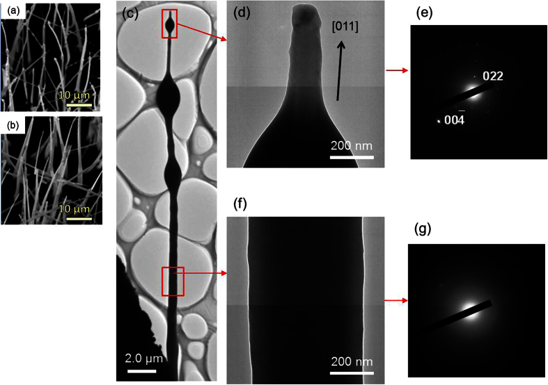
Figure 4.
SEM images of nanowires grown at (a) 1250 °C and (b) 1300 °C. (c–g) TEM images of a bent nanowire with lumps, and the electron diffraction patterns; (c) whole image of the nanowire, (d) an enlarged view of the tip of the nanowire, and (e) the electron diffraction pattern recorded along the [ ] zone axis from the tip of the nanowire. (f) The enlarged view and (g) the electron diffraction pattern of the middle section of the nanowire.

