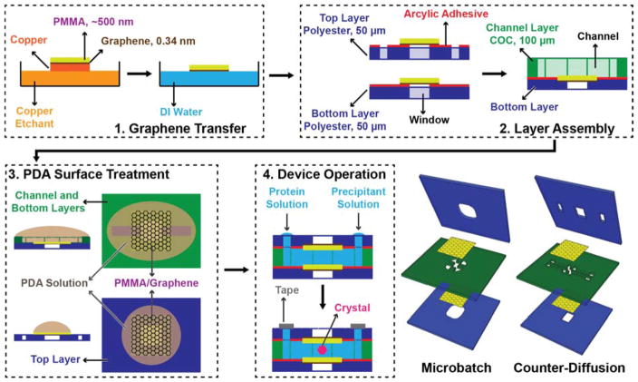
Fig. 2.
Schematic depiction of the fabrication scheme for thin-film graphene-based microfluidics, using a channel-based counter-diffusion as the example. (1) CVD-grown graphene on copper is first coated with a layer of PMMA, and then released from the copper substrate by etching. The subsequent film is floated on the surface of water for (2) transfer to an adhesive polyester support layer to define the window areas of the device. This layer is then adhered to a COC layer containing the cut-out pattern for the microfluidic channels. (3) A hydrophilic PDA surface treatment on both the top PMMA/graphene film and the bottom layer containing the microfluidic channel facilitates easy filling of the final device via capillary action. (4) The final, assembled device is held together by the adhesive layers defining the window structures, leaving the PMMA/graphene window areas free of excess material. Either microbatch or counter-diffusion crystallization trials can be set up by the addition of protein and precipitant solutions. The device inlets are sealed with Crystal Clear tape.

