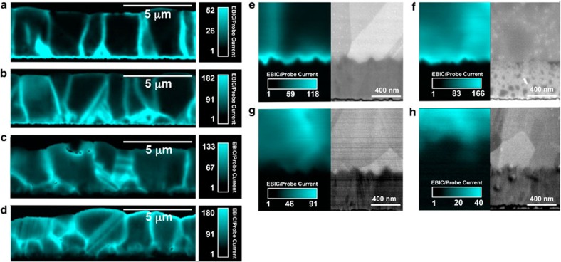
Figure 2. Cross-sectional EBIC maps.
(a–h) Cross-sectional EBIC maps of the devices prepared with (a) 50, (b) 100, (c) 200 and (d) 400 nm-thick CdSe layers. The associated contrast bars represent the EBIC current divided by the probe current (no units). SE-SEM images and simultaneously acquired EBIC maps of the devices with (e) 50, (f) 100, (g) 200 and (h) 400 nm CdSe layers. The 50 and 100 nm CdSe layers do not have small CdSe grains interfacing the FTO, while the 400 nm sample shows small CdSe grains interfacing the FTO. The EBIC map combined with the SE-SEM image for the 400 nm CdSe layer sample (h) shows that the small CdSe grains interfacing the FTO are not photoactive.

