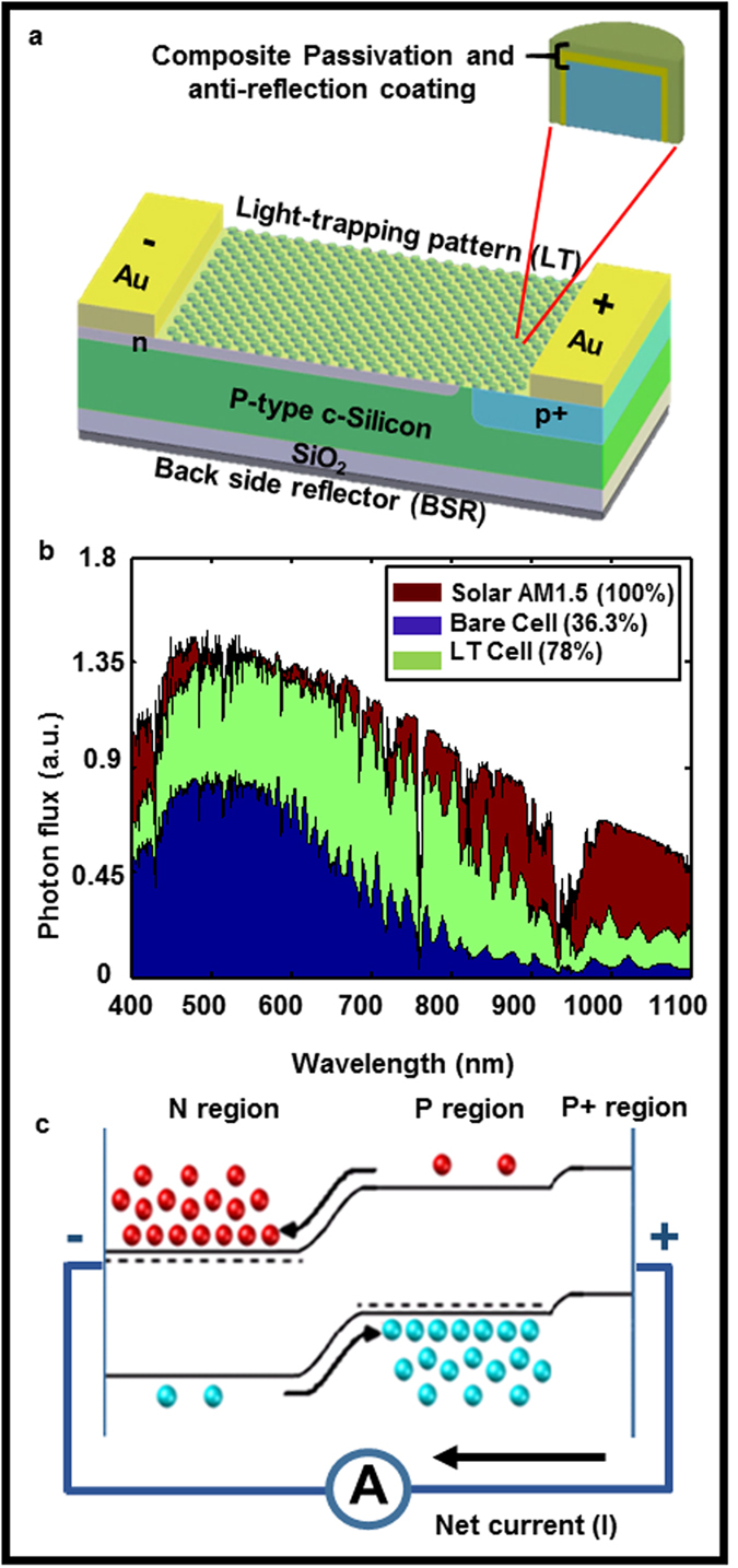
Figure 1. Device schematic, optical absorption, and band diagram.

(a) Illustrates the c-Si solar cell architecture which combines the light trapping scheme with the functional cell geometry. (b) The absorbed photo flux as a function of wavelength with reference to AM1.5D solar spectrum for bare and light trapping cell inside a 3 μm thick wafer and (c) the corresponding band diagram under illumination.
