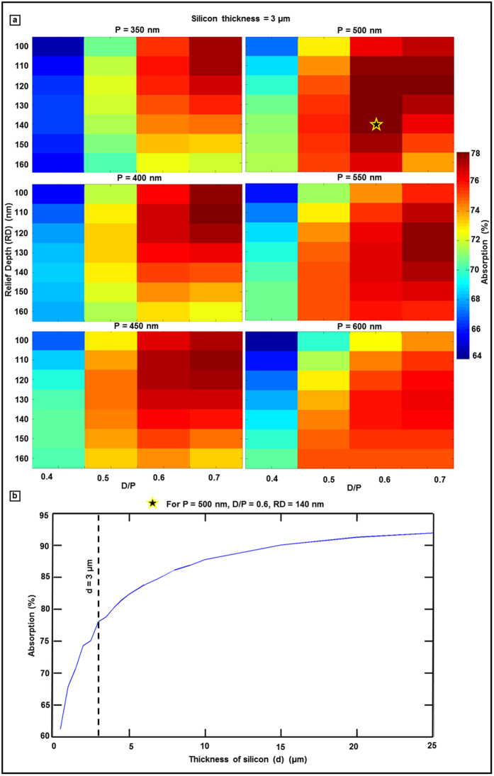
Figure 2. Light trapping pattern dimension and Si thickness optimization.
(a) FDTD predicted light trapping pattern optimization for a constant silicon thickness (3 μm). The wavelength integrated absorption is maximized as a function of 2D hexagonal lattice period, D/P and relief depth. (b) Silicon absorption as a function of silicon thickness for the optimized light trapping pattern (P = 500 nm, D/P = 0.6, RD = 140 nm with ARC (SiO2/SiN = 50/35 nm)).

