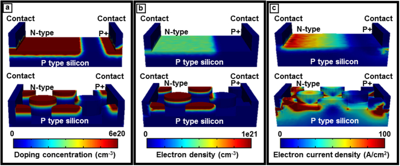
Figure 4. Doping and charge carrier generation profile.
(a) The doping profile of the 3 μm thick silicon cell with and without light trapping. The p and n regions are defined which show the gradient of impurities in the device. (b) Compares the electron density of a 3 μm bare cell with light trapping cell. The electron density in n-type region of the light trapping cell is higher than that of the bare cell, and (c) shows the corresponding electron current density. The structure geometries in this figure are not to scale. The color bar upper and lower limits are chosen in order to enhance the contrast.

