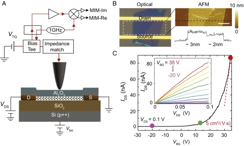
Fig. 1.
Experimental setup and device characterization. (A) Schematic diagram of the device and the MIM setup. The 1-GHz microwave signal is guided to the tip through an impedance match section, and the reflected signal is detected by the MIM electronics. The carrier density can be either globally tuned by the back-gate voltage VBG or locally modulated by the dc bias on the tip VTG. (B) Optical and the zoom-in AFM images of an exfoliated MoS2 FET device. (Inset) A line profile across the surface. (Scale bar, 5 μm.) (C) Transfer characteristics of the device at VDS = 0.1 V. The dashed line is a linear fit to the curve for VBG > 30 V, from which the field-effect mobility μFE ∼ 5 cm2/(V⋅s) can be deduced. The solid circles (purple, green, and red) match the color coding in Fig. 5. (Inset) The output characteristics from VBG = 35 V to −20 V with 5-V steps.

