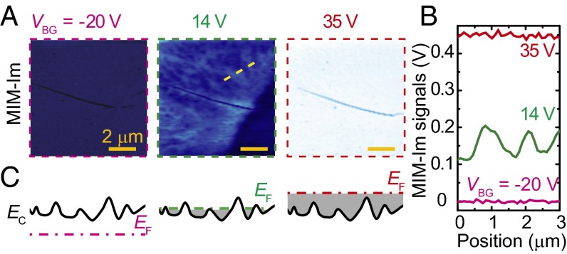
Fig. 5.
Electrical inhomogeneity in the MoS2 FET device. (A) Close-up MIM-Im images in the center of the flake at VBG = −20 V, 14 V, and 35 V. (Scale bars, 2 μm.) (B) Line cuts along the orange dashed line in A at the three VBG as in A. (C) Schematics of the relative positions between EF and the spatially fluctuating EC at the same VBG as in A and B. The color coding (purple, green, and red) matches the solid circles in Fig. 1C.

