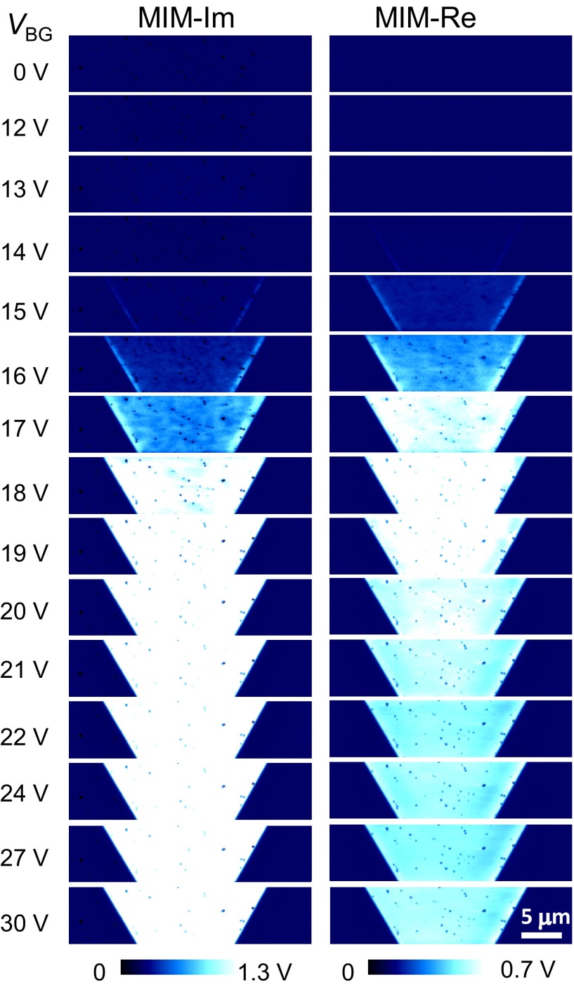
Fig. S3.
MIM-Im (Left) and MIM-Re (Right) images of a device fabricated on a CVD-grown MoS2 flake at different back-gate voltages. The overall evolution of MIM signals as a function of VBG, the emergence of edge states (e.g., at VBG = 14 V), and the conductance inhomogeneity (e.g., at VBG = 17 V) are again observed in this sample. Note that different color scales compared with the data of exfoliated sample are adopted here for better visualization, because a different MIM tip was used and the MIM contrasts were different. For different tips, a calibration on standard sample and Im/Re are used for quantitative analysis (46).

