Figure 2.
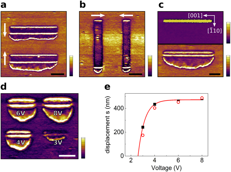
(a–c) PFM images of PST ferroelectric layer, scale bars are 1 μm, vertical scale is in a.u. for PFM amplitude and 360° for PFM phase, crystallographic directions displayed in (c) are representative for all PFM images. (a,b) Lateral PFM amplitude images of poled regions, different slow scan directions of the tip are represented by white arrows. The secondary domain always appears at the same side, towards the [ ] direction. (c) Vertical PFM phase (top) and lateral PFM amplitude (bottom) images of a switched line, switching was done at a scan speed of 100 nm/s. (d) Lateral PFM amplitude image of regions poled with different voltages as shown in the image. Scale bar is 500 nm. (e) Measured (squares and dots) and extrapolated (full line) displacement of the CDW as a function of the applied switching voltage.

