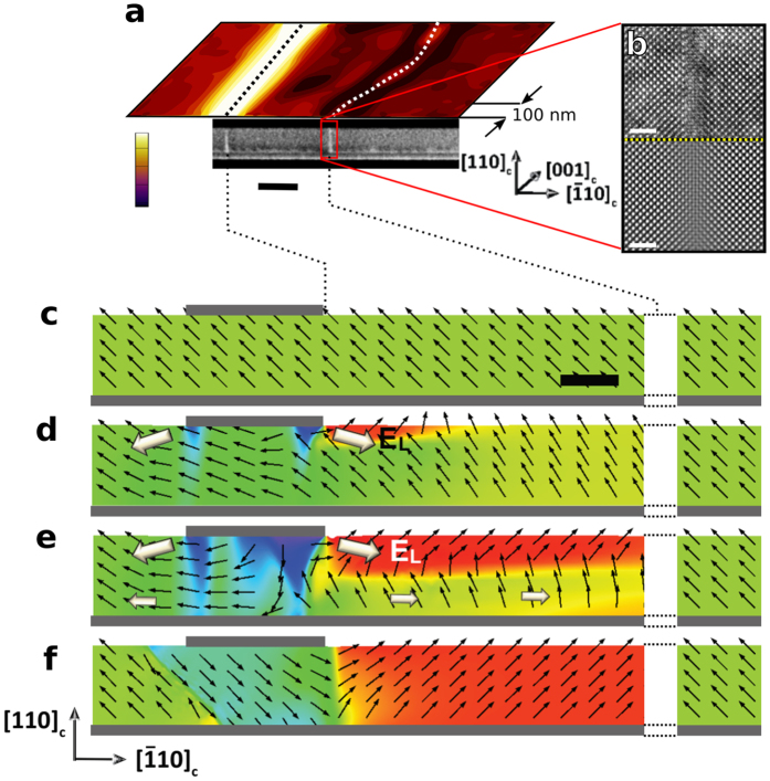
Figure 3.
(a) Lateral PFM amplitude and the corresponding TEM image of a poled region in the PST ferroelectric layer, both set to the same scale. Scale bar is 100 nm, vertical scale of PFM amplitude in a.u. Domain walls are indicated by dotted lines. (b) HRTEM (upper panel) and corresponding Fourier filtered image (lower panel) of the CDW present between the secondary domain and the non-switched area. Scale bar is 2 nm. (c–f) Phase field simulation of the switching process. Scale bar is 40 nm. The black arrows represent the local ferroelectric polarization direction. The simulation spans only a small area, farther away on the right would be the original polarization direction again. (c) As grown single domain state. (d) The applied dc bias voltage between the top and bottom electrodes (gray lines) initiates 180° switching under the electrode and nucleates side domain by in-plane 90° switching on the side of the top electrode. (e) The in-plane electric field due to the limited conductivity of LSMO and the charge transfer propagates the secondary domain. (f) Completed stable domain structure after the dc bias voltage is removed.

