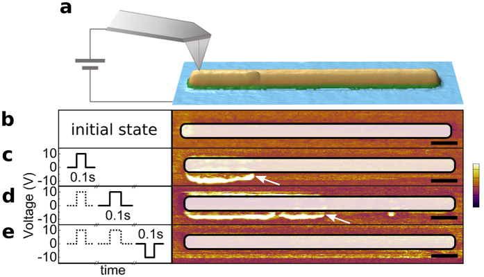
Figure 4.
(a) AFM topography image of a Pt electrode with dimensions of l × w × h = 5000 × 250 × 4 nm3 deposited on the PST film and representation of the tip position for the switching procedure. (b–e) Application of switching pulses on the top electrode (left) and the resulting lateral PFM amplitude images (right). Scale bars are 500 nm, vertical scale of PFM amplitude in a.u. (b) The film exhibits a homogeneous polarization in the initial state. (c) Due to 180° switching below the electrode, a secondary domain is created (white arrow). (d) Repeating the same pulse causes the secondary domain to move further. (e) Application of opposite voltage resets original state, the secondary domain is fully erased.

