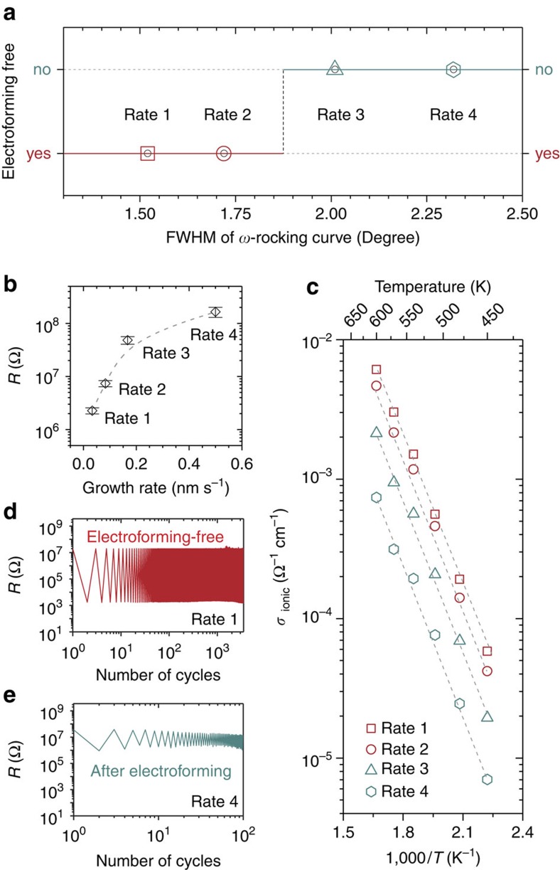
Figure 7. Electronic and ionic transport properties of VHN deposited from different film growth rates.
(a) Electroforming-free resistive switching properties of SDC:STO VHN films depending on full width at half maximum (FWHM) values in ω-rocking curves; Rate 1 (red square); Rate 2 (red circle); Rate 3 (turquoise triangle); Rate 4 (turquoise hexagon). (b) Resistance values of the pristine states of the device with SDC:STO VHN films deposited from different growth rates (read voltage: 0.2 V). Error bars are provided as s.d. (c) Temperature-dependence of ionic conductivity (σionic) for SDC:STO VHN films deposited from different growth rates. (d,e) Resistance variation with repeated electrical cycles (with applied voltages of –5 and +5 V for switching and a read voltage of –0.3 V) of SDC:STO VHN film devices with different growth rates.

