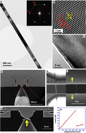
Fig. 1. Sample and experimental configuration.

(A) VLS-grown Si nanowire sample with a uniform diameter of ~100 nm. Inset: Selected area electron diffraction (SAED) pattern indicates that Si nanowire is a single-crystal cubic diamond structure grown along the <110> orientation, which has been confirmed by the corresponding high-resolution transmission electron microscopy (HRTEM) image. (B) Lattice spacing of ~0.19 nm with respect to the <110> plane of Si. (C) HRTEM side view of a Si nanowire showing the atomically smooth surface. (D) In situ scanning electron microscopy (SEM) tensile testing of a single nanowire based on a push-to-pull MMD actuated by an external quantitative nanoindenter. (E to G) Zoom-in views (G) of the yellow frame in (D) are presented in (E) and (F), showing the detailed clamping configuration of a single nanowire sample at a lower voltage of 2 kV (E) and a regular working voltage of 20 kV (F). The tensile gauge length is indicated by the red bar in (E), whereas the yellow arrows in (F) indicate the uniaxial tensile loading direction. (H) Typical load-versus-displacement curve read from the nanoindenter for a monotonic tensile test under the displacement control mode. The abrupt force drop indicates the failure of the nanowire sample.
