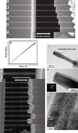
Fig. 2. In situ SEM tensile tests and postmortem TEM analysis.

(A to F) Elongation of a single Si nanowire (diameter, ~86 nm). (A) Original status before test. (B to E) Extracted frames show gradual elongation of Si nanowire under tensile straining, with a maximum strain of 13% just before fracture (E). (F) Most of the nanowires flew away right after fracture, except the clamped portion. (G) The corresponding stress-versus-strain curve is nearly linear, with a fracture stress of ~16 GPa. (H and I) Loading-unloading test with increasing tensile strain amplitude and full unloading in each cycle. (H) Si nanowire before test (diameter, ~120 nm). (I) Loading–fully unloading process, in which the nanowire fully recovers its original length after strain values of ~5.8, ~8.1, ~9.7, and 13.2% are experienced. The nanowire finally broke at the fifth cycle with a strain value of ~13.5%, with one piece of broken nanowire remaining on the stage (as marked in the white frame); note that there is a thin, nonuniform layer of glue coating the nanowire [the red dashed lines in (H) indicate the true nanowire boundary]. (J and K) Bright-field TEM images showing a typical brittle fracture surface morphology, in which the nanowire remained in the single-crystalline structure [inset SAED pattern in (K)] with a uniform diameter [highlighted by red dashed lines in (J), with a small amount of conductive epoxy glue over the surface] and a flat fracture surface. All the images in (J) and (K) were taken in <1-11> zone axis. (L) The HRTEM image of the front end of the nanowire fracture surface [the red rectangular area in (K)] shows the single-crystalline structure with flat fracture surface (highlighted by red dashed lines); during the sample transfer and posttesting TEM analysis, a thin layer (~5 to 6 nm) of amorphous silicon oxide was formed at the fracture surface (L) with no visible sign of plastic deformation.
