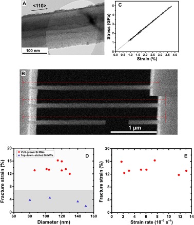
Fig. 4. Comparison between VLS-grown Si nanowires and top-down etched Si nanowires.

(A) Bright-field TEM showing a top-down etched single-crystal Si nanowire (also in <110> orientation) with a uniform diameter but a relatively rough surface. (B) Deformation process of a top-down etched Si nanowire upon tensile straining (diameter, ~140 nm) with the corresponding stress-versus-strain curve. (C) Si nanowire broken in an elastic manner with a fracture strain of ~3.7% (fracture stress, ~5 GPa; calculated Young’s modulus, ~135 GPa). (D) Summary of the comparison for the fracture strain versus nanowire (NW) diameter between the VLS-grown (red dots) and top-down etched (blue triangles) Si nanowires. The shaded bottom area indicates the range of previously reported tensile strain values for Si nanowires with diameters of >20 nm (25–27). (E) Summary of the fracture strains of VLS-grown Si nanowires versus their strain/loading rates, indicating that the elastic limit is insensitive to strain rate in this range.
