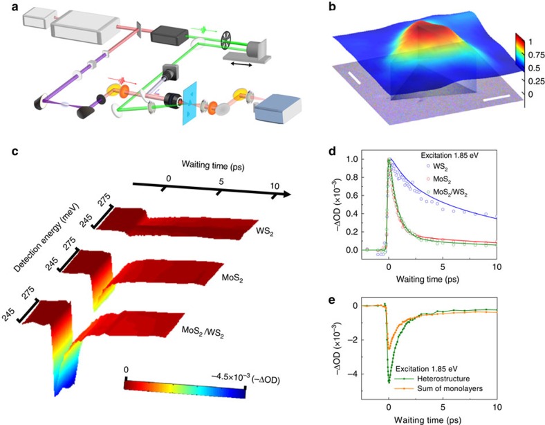
Figure 2. Ultrafast visible/IR microspectroscopy measurements.
(a) A schematic illustration of ultrafast visible/IR microspectroscopy. (b) Image of transient absorption change for a 100 × 100 μm area of MoS2/WS2 heterostructure sample. The bottom layer of the figure is the optical image of the measured area, where the heterojunction is located at the centre. Scale bar, 20 μm. The top layer represents the transient absorption change 100 fs after the excitation of MoS2 with a pulse centred at 1.85 eV. The intensity of signal from the MoS2/WS2 heterojunction region is about twice of that from MoS2-only region. (c) Temporal evolutions of the 670 nm (1.85 eV) excitation-induced absorption changes detected at 0.245–0.275 eV of MoS2, WS2 and the MoS2/WS2 heterostructure. OD, optical density. (d) Normalized plots of (c) detected at 0.25 eV (2,000 cm−1). Dots are data, and curves are multi-exponential fitting with the consideration of instrument response function (IRF). (e) The signal of the MoS2/WS2 heterostructure and the signal sum of the two individual MoS2 and WS2 monolayers. The initial intensity of the heterostructure is nearly 100% larger than the signal sum of the two monolayers. All measurements were made at room temperature with incident pump fluence ∼80 μ J cm−2. The photo-excited carrier densities is ∼1012–1013 carriers per cm−2.

