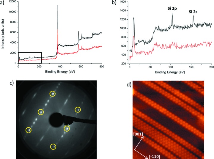
Figure 8.
Different techniques measured in situ in the same chamber for studying a sample of silicon nanoribbons grown on an Ag(110) substrate. (a) XPS spectra showing signals collected for clean Ag(110) (red line) and after <1 monolayer Si deposition. (b) XPS close-up view labelling the additional peaks due to Si. (c) Low-energy electron diffraction pattern showing a (5 × 2) superstructure. The pattern was collected at 70 eV and the integer order spots are highlighted with yellow circles. (d) STM image showing the characteristic nanoribbon structures [200 nm × 200 nm, V(t) = 1 V, I(t) = 50 pA].

