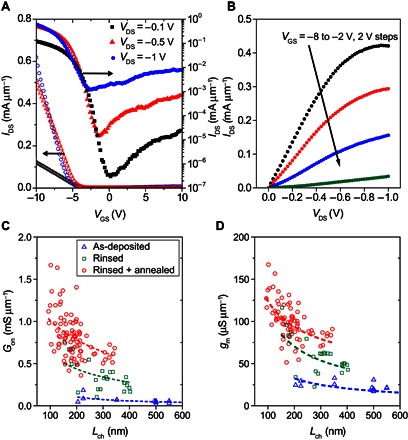
Fig. 2. Electrical properties of CNT array FETs and influence of postdeposition treatment on conductance.

(A) IDS-VGS curves forward sweep for a representative “rinsed + annealed” FET with Lch = 100 nm where the open and filled symbols are plotted on linear and logarithmic scales, respectively. (B) IDS-VDS output curves for the same device as in (A). (C) Gon versus Lch obtained from CNT arrays that have undergone the three different postdeposition treatment conditions, fit to Eq. 1, with a sevenfold total increase in Gon resulting from the “rinsed + annealed” treatment. (D) gm versus Lch for each surface treatment fit to as a guide to the eye, with a threefold total increase in gm resulting from the “rinsed + annealed” treatment.
