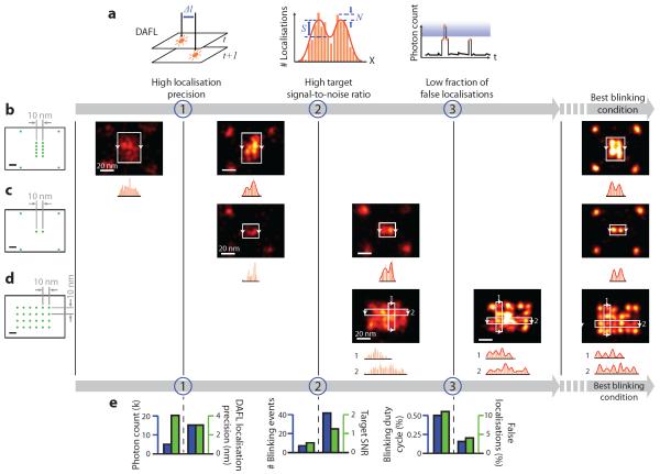
Figure 2. Systematic characterisation of blinking requirements and optimisation of DNA-PAINT imaging quality.
(a) Methods for systematic characterisation of the three blinking requirements depicted in Fig. 1. (1) Distance between adjacent-frame localisations (DAFL) measures distance between pairs of spatially-close localisations originated from adjacent camera frames. (2) Target signal-to-noise ratio (target SNR) measures separability of peaks in localisation histogram, in the super-resolved image. S, signal; N, noise; red curve indicates two-peak Gaussian fit. (3) Photon count cut-off in blinking trace measures fraction of false localisations. Blue shaded area indicates identified false localisations. Orange markers, bars and curves indicate localisations, histograms and time traces, respectively.
(b-d) Designed origami standards with 10 nm spacing under different blinking conditions. Leftmost column, design schematics of DNA origami standards; green dots indicate DNA-PAINT docking strands; four corners in (b) and (c) are used as alignment markers. Right five columns, DNA-PAINT images under increasingly better blinking conditions (one condition per column). Histograms below images show projection profiles from the areas indicated by white boxes and projected along the directions of arrows.
(e) Quantitative characterisation and pairwise comparisons of imaging conditions used in (b-d), before and after meeting each additional requirement, assayed with methods in (a). For each comparison, left axis (blue) shows the control parameter and right axis (green) shows experimental measurement.
For more details, see Supplementary Figures S3-S5 on origami designs, Supplementary Figures S6-S13 for super-resolution images, online methods and Supplementary Methods S3, S5 for DNA-PAINT imaging conditions and analysis methods. Scale bars, 10 nm in schematics and 20 nm in super-resolution images.

