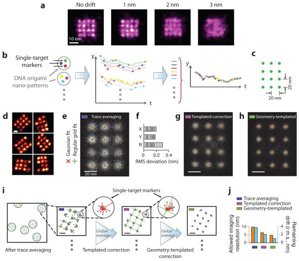
Figure 3. Principle and performance of DNA nanostructure templated drift correction.
(a) Effect of drift on imaging quality, simulated for the biomolecular complex in Fig. 1a with 1 nm localisation precision and different levels of stage drift. Only with 1 nm (r.m.s.) or less drift can the structure be clearly visualised.
(b) Principle of templated drift correction method with pre-designed nanostructure patterns. Illustrated with a three-target marker example, schematics show nano-pattern design with single-target markers (left), localisation time traces from individual single-target markers (middle), and averaged drift correction trace after combining traces from many markers (right). Targets and traces are colour-matched.
(c) Design schematics of a 3 × 4 square grid with 20 nm point-to-point spacing on a DNA origami nanostructure. Each green dot indicates a docking strand.
(d) Representative DNA-PAINT super-resolution images of the 20 nm grid structure in (c), imaged with 300 ms frame time, 30,000 total frames, and 3 nM imager strands. Missing grid points were likely due to synthesis or incorporation defects (see Supplementary Notes S9.1 for more discussions).
(e) Single-particle averages of 20 nm grid images (N = 700) after trace averaging. Overlaid crosses indicate Gaussian fitted centres (red) and regular grid-fitted centres (green) using the red crosses as fitting targets.
(f) Root-mean-square (r.m.s.) deviation between the Gaussian fitted and regular grid-fitted centres in (e).
(g, h) Single-particle averages of 20 nm grid images (N = 700) after templated (g) and geometry-templated (h) drift correction. Overlaid crosses indicate Gaussian fitted (red) and regular grid-fitted centres (green) as in (e). The same colour code for different stages of drift correction in (e), (g), (h) are also used in (i), (j) and Fig. 4.
(i) Procedure for templated and geometry-templated drift correction with 20 nm grid structures as templates. Schematics shows a large field-of-view image with many drift markers, after simple trace averaging (leftmost). Each grey circle indicates a 20 nm drift marker. Zoomed-in (square) schematics shows a super-resolved 20 nm grid marker, after simple trace averaging (left), after templated drift correction (middle), and after geometry-templated correction (right). Further zoomed-in schematics (round) shows one single-target marker and calculation of offset vectors. In zoomed-in schematics (square and round), grey dots indicate localisations, green dots and lines indicate Gaussian-fitted centres and regular grid-fitted lattices as guides for templated and geometry-templated drift correction calculation, red line segments with arrowheads represent calculated offset vectors.
(j) Comparison of allowable imaging resolution (measured in FWHM, blue) and estimated remaining drift (green) at different stages of drift correction.
For more details, see online methods and Supplementary Methods S2, S5 for simulation and analysis methods, Supplementary Figures S14 for super-resolution images. Scale bars: 10 nm in (a), 20 nm in (d-f) and zoomed-in images in (i).

