Figure 3.

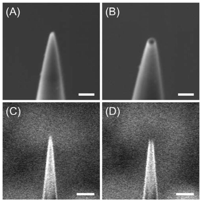
SEM images of (A) unmilled and (B) FIB-milled carbon nanotips and the corresponding FIB images in parts C and D, respectively. Scale bars: 200 nm in parts A and B, and 500 nm in parts C and D.

SEM images of (A) unmilled and (B) FIB-milled carbon nanotips and the corresponding FIB images in parts C and D, respectively. Scale bars: 200 nm in parts A and B, and 500 nm in parts C and D.