Figure 7.

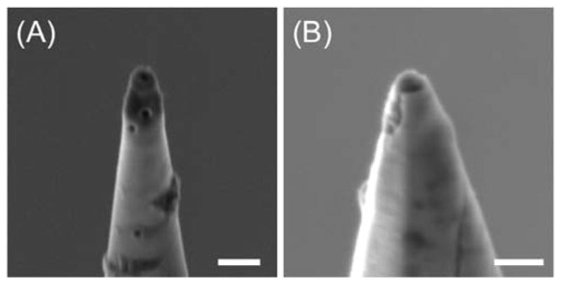
SEM images of (A) unmilled and (B) FIB-milled carbon nanotips with ESD damage. The latter tip was used for CV measurements in the bulk solution before SEM imaging. Scale bars: (A) 500 nm and (B) 200 nm.

SEM images of (A) unmilled and (B) FIB-milled carbon nanotips with ESD damage. The latter tip was used for CV measurements in the bulk solution before SEM imaging. Scale bars: (A) 500 nm and (B) 200 nm.