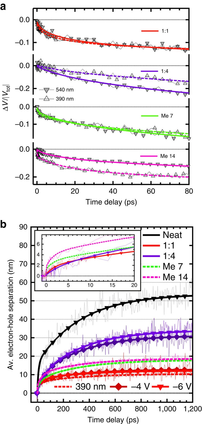
Figure 4. Analysis of the EDA data.
(a) Normalized voltage drop dynamics (ΔV/|Vtot|) obtained from the EDA decay for the different investigated pBTTT:PCBM devices (see legend), at a reverse bias of −6 V, with excitation at 390 (empty triangles, dashed fit curve) or 540 nm (full downward triangles, smooth fit curve) at a fluence within the linear photocurrent regime. (b) Average electron–hole separation calculated from the voltage drop dynamics across the devices shown in the legend, at an applied bias of −6 (full downward triangles) or −4 V (full diamonds). Dashed lines are for 390 nm excitation (at −6 V) and smooth lines for 540 nm excitation. The inset zooms on the first 10 ps. Best sum of exponential fits are shown as thick lines.

