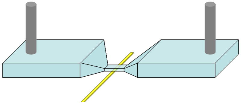
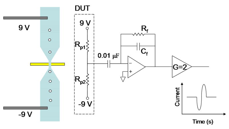
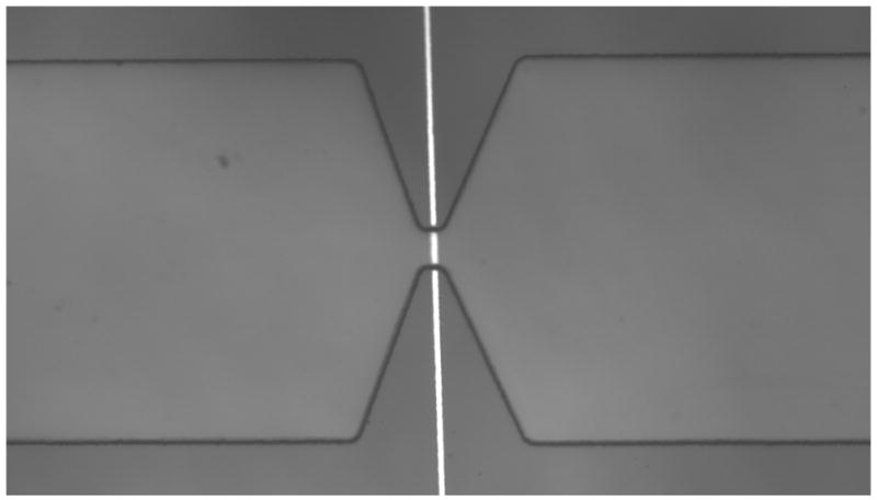
Figure 1.


(a) Schematic of microfluidic device integrated with open circuit electrode at the bottom surface of the micropore. Microchannels 300 μm wide taper down to smaller pore so that majority of voltage drop is across the pore. Positive and negative voltage applied at outer channel edges. (b) Circuit diagram of device under test (DUT) integrated with readout electronics. Transient change in current across the pore is amplified using integrator circuit configuration. (Inset) Bead passing through the pore results results in drop in current and then rise. (c) Optical micrograph of fabricated microdevice. Electrode is fabricated on glass substrate. Microchannel on top is embedded in PDMS.
