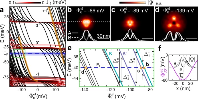
Figure 4.
(a) Tight binding
eigenenergies of a 120 × 100 nm 2 graphene sample
with open boundaries as a function of tip-induced potential amplitude
Φ0el at B = 7 T with the tip-induced potential centered on an AB
area (BA and AA yield very similar behavior, not shown). Line color
encodes coupling to the boundary (imaginary part Γl of eigenenergies); black (red) indicates strong
(weak) localization underneath the tip. States from LL±1 and the split LL0 are labeled by ±1 and 0, respectively.
The LL0 splitting reduces the confining gap to E0– – E–1 ≈ 50 meV. First states crossing EF from LL±1 are highlighted
in orange. Uncertainty in EF indicated
as blue horizontal bar (Supporting Information). The green rectangle marks the zoom shown in panel e. (b–d)
Color plot of the wave function amplitude  of states marked by
orange crosses in panel e. Φ0 at the crossing point εl(Φ0el) = EF is marked.
Solid (dashed) white lines are line cuts along the dotted white line
in panel b for contributions from sublattice A (B), as marked. All
scale bars identical. (e) Zoom into area marked by a green box in
panel a. Colored lines identify valley K (cyan) and K′ (purple).
Orange crosses mark crossing of EF (blue
dashed line) of selected states, which are displayed in panels b–d.
First two orbital Δj and valley Δkτ splittings
marked by arrows. (f) Comparison of length scales: tip-induced potential,
magenta; calculated wave function amplitude |Ψ| of first state
crossing EF (same as panel b) for sublattice
A (gray line) and B (dashed line); superstructure lattice constant a = 13.8 nm; magnetic length lB (7 T) = 9.7 nm.

