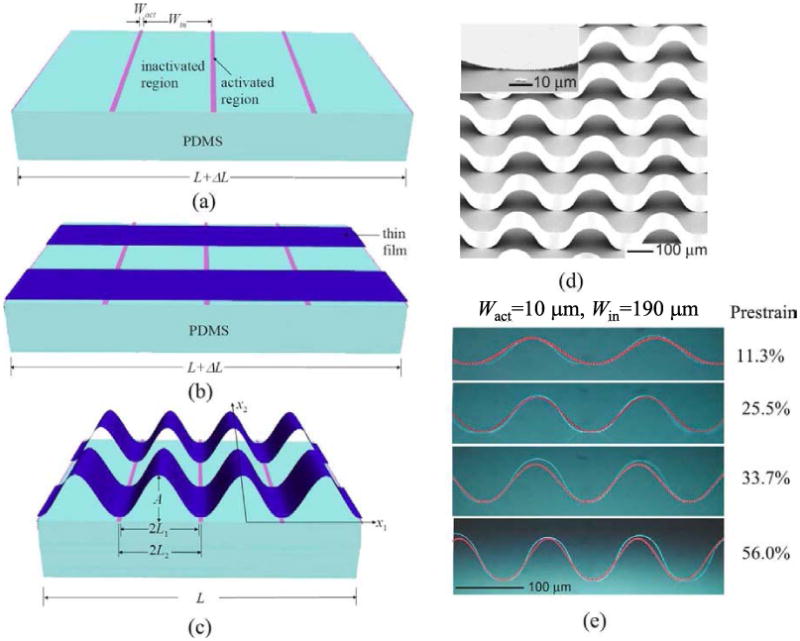
Fig. 4.

(a) Prestrained PDMS with periodic activated and inactivated patterns. (b) Thin film parallel to the prestrain direction is attached to the prestrained and patterned PDMS substrates. (c) Relaxation of the prestrain in the PDMS leads to buckles of the nanoribbons. (d) SEM image of buckled GaAs nanoribbons formed using (a)–(c). Inset: GaAs/PDMS substrate interface. (e) Buckled GaAs thin films on patterned PDMS substrate for different prestrain levels: 11.3%, 25.5%, 33.7%, and 56.0% (from top to bottom). The red lines are the profiles of the buckled GaAs thin film predicted by the analytical solution. (Reprinted with permission from [22].)
