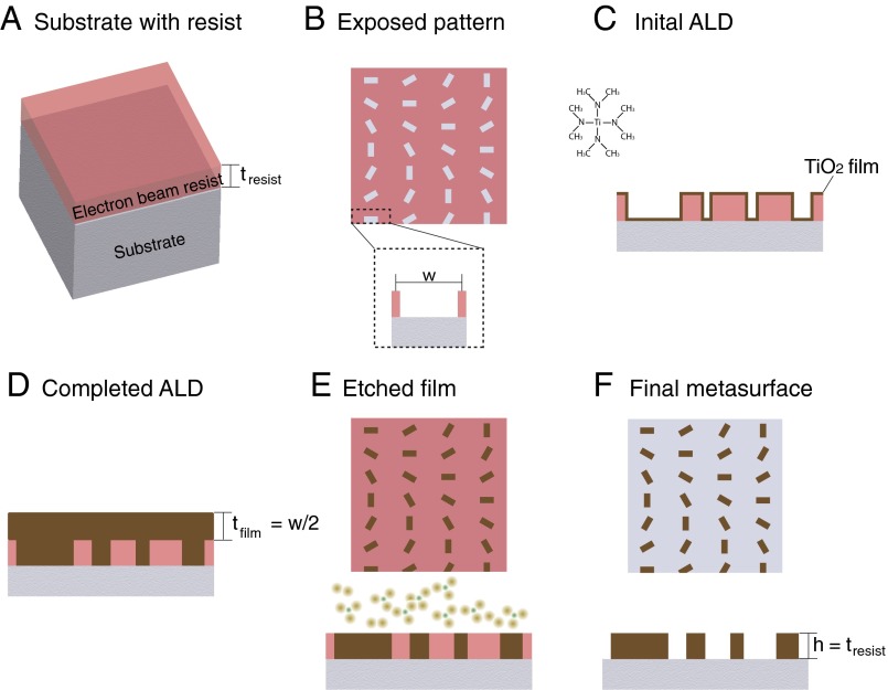
Fig. 2.
Fabrication process for DMs. (A) EBR on fused silica (or equivalent transparent substrate) with thickness tresist that ultimately sets the height of the final structure (perspective view). (B) Inverse of the final metasurface pattern imprinted into the EBR by electron beam lithography and subsequent development of the pattern (top view). The boxed area is an expanded cross-section of the maximum feature width, w. (C) Initial TiO2 deposition via ALD conformally coats sidewalls and top of the EBR and exposed substrate (side view). TDMAT molecule used for ALD is also shown. (D) Completed deposition of the TiO2 yields a film thickness greater than half the width of the maximum feature size, tfilm ≥ w/2. (E) Exposed tops of the TiO2 metasurface and residual EBR after reactive ion etching with a mixture of Cl2 and BCl3 ions (top and side view). (F) Final DM after removal of remaining EBR (top and side view).

