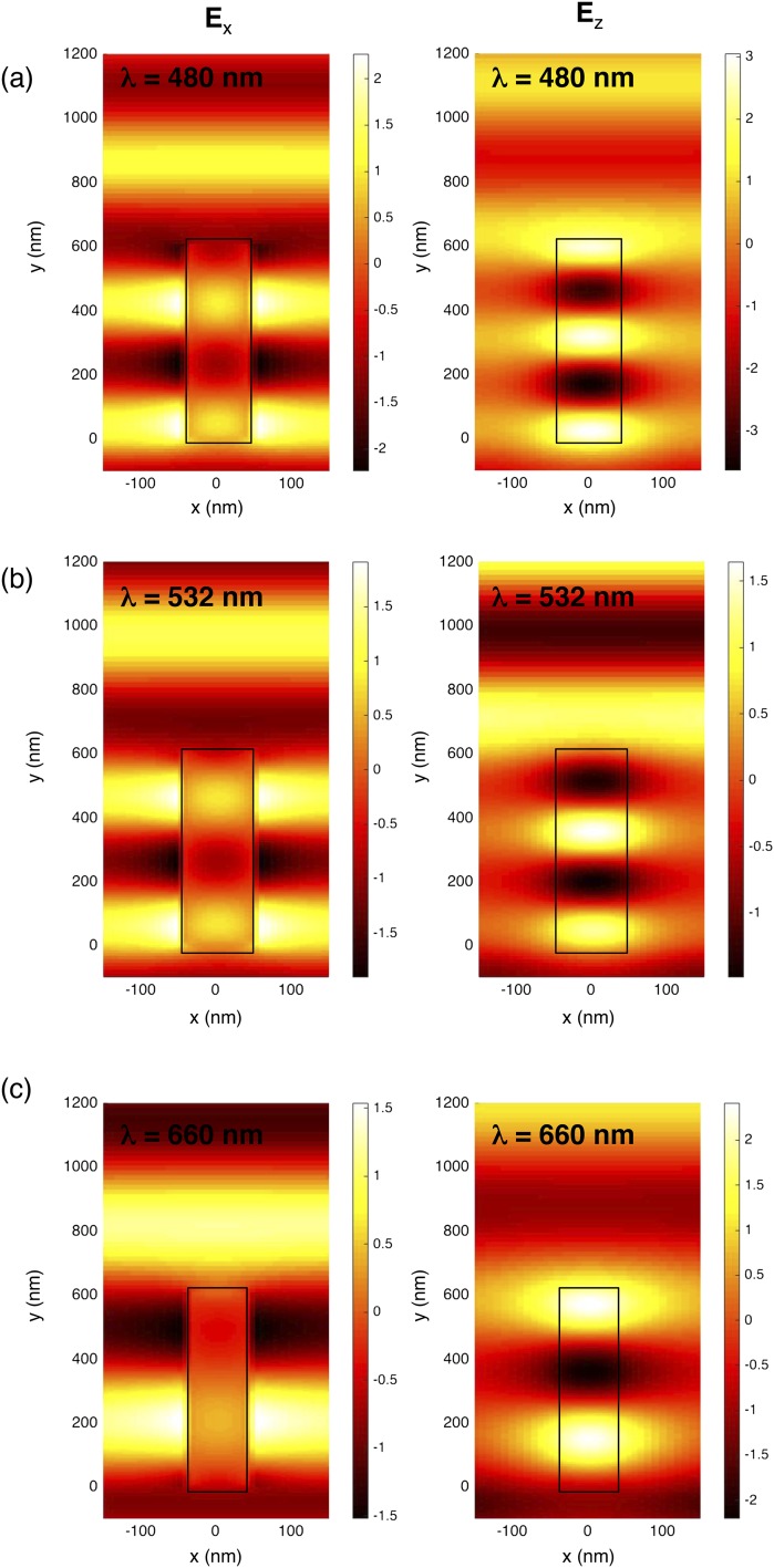
Fig. S5.
Simulated electric field profiles at design wavelength. Real part of the x component (Left) and z component (Right) of the electric field at design wavelengths (A) 480 nm, (B) 532 nm, and (C) 660 nm. All fields are shown through a cross-section of the nanofin width, and the nanofin is highlighted in each panel with a black box. One can see that the x and z components of the electric fields exiting the pillar, at each wavelength, are out of phase by π radians, as required for PB phase. The TiO2 pillars are simulated on a glass substrate that occupies the half space below y = 0, and the wave propagates in the +y direction.

