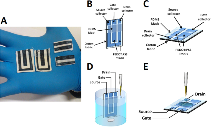
Figure 2. Device pictures and experimental setup.
(A) Pictures of screen printed OECTs obtained in the conformation G1 (1) and G2 (2). (B) Scheme of OECT in G1 geometry. (C) Scheme of OECT in G2 geometry. (D) Scheme of experimental apparatus for G1 transistor. (E) Scheme of experimental apparatus for G2 transistor.

