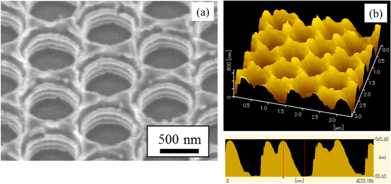
Figure 4.
(a) SEM image of the sample after four repeated etching steps using resist and SiO2 interlayer as a mask. The etching depth is set to 100 nm for each step. (b) SPM image of the sample after six repeated etching steps using resist and SiO2 interlayer as a mask. The depth of 490 nm is obtained.

