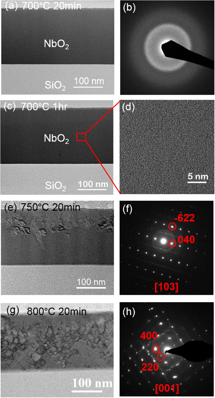
Figure 2. Microstructural evolution in NbO2 thick film as the function of annealing temperature.
(a) BF cross-sectional TEM image and (b) SAED pattern at 700 °C; (c) BF image and (d) SAED pattern from NbO2 with distorted rutile phase along [103] at 750 °C; (e) BF image and (f) SAED pattern from NbO2 with distorted rutile phase along [001] at 800 °C.

