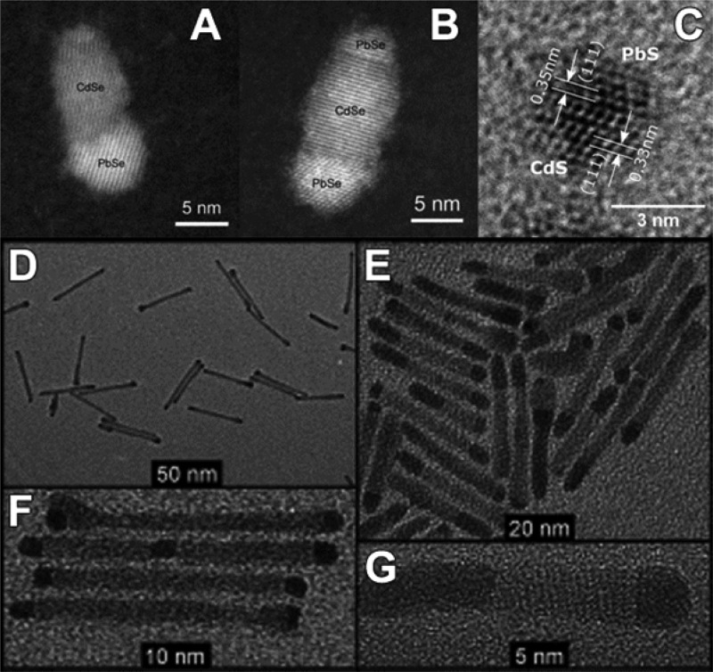
Figure 18.
(A,B) HAADF images of w-CdSe/rs-PbSe NRs obtained with Cd-to-Pb partial conversion of CdSe NRs. The NHC have either only one or both tip converted into PbSe, in the latter case with different extents of conversion. The resulting clear PbSe/CdSe interfaces are parallel to the (0001) plane of w-CdSe. Reproduced from [Lee, D.; Kim, W. D.; Lee, S.; Bae, W. K.; Lee, S.; Lee, D. C. Direct Cd-to-Pb Exchange of CdSe Nanorods into PbSe/CdSe Axial Heterojunction Nanorods Chem. Mater. 2015, 27, 5295–5304]. Copyright 2015 American Chemical Society. (C) Janus-like spherical NC where approximately half of each QD is made PbS and half is CdS. The resulting c PbS/CdS interface is parallel to the (111) plane of both cubic structures. Reproduced from [Zhang, J.; Chernomordik, B. D.; Crisp, R. W.; Kroupa, D. M.; Luther, J. M.; Miller, E. M.; Gao, J.; Beard, M. C. Preparation of Cd/Pb Chalcogenide Heterostructured Janus Particles via Controllable Cation Exchange ACS Nano 2015, 9, 7151–7163]. Copyright 2015 American Chemical Society. (D–G) CdS/Pd4S hybrid nanostructures: (D) tip growth of Pd4S on 5.9 nm diameter nanorods; (E) more extensive growth of Pd4S on a sample of CdS nanorods with a broad size distribution; (F) close-up of the sample shown in (D); (G) HRTEM of a single CdS/Pd4S NR from the sample shown in (E). Adapted with permission from ref (191). Copyright 2010 John Wiley and Sons.

