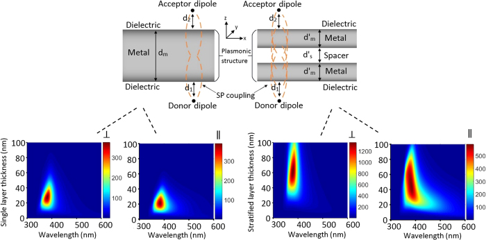
Figure 1. Single layer and stratified nanostructures and enhancement factor.
Architectures of the single layer (a) and stratified (b) plasmonic nanostructures. The donor dipole is placed at one side of the plasmonic layer (single metal film or stratified metal-dielectric layers) and the acceptor dipole is at the opposite side. The surrounding media are isotropic and non-absorbing. Calculated electric field enhancement factor at the acceptor dipole position as the functions of plasmonic layer thickness and excitation wavelength for simple (c,d) and stratified (e,f) nanostructures and theoretical steady state efficiency. The dipole moment is oriented perpendicular (c,e) and parallel (d,f) with respect to the plasmonic layer surface. The donor/acceptor dipole distance to the nearest plasmonic layer surface is 10 nm and the equation  is applied for the single layer and stratified configurations.

