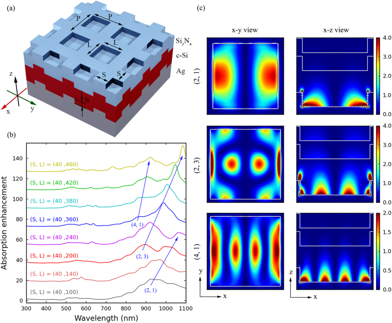
Figure 1.
(a) Schematic of the simulated structure. The ring-shaped nanocavities on the Ag bottom layer are arranged in a square lattice, with lattice constant P, side length L, depth h and ridge width S = P − L. Then, the subsequent 100 nm c-Si and 50 nm Si3N4 layers are textured conformally, forming the absorption enhancement design. (b) Absorption enhancement for nanocavity arrays with fixed S = 40 nm and different L’s as a function of wavelength, relative to the corresponding bare structure. These curves are offset for clarity. (c) Patterns for |Ez|2 component of the electric field in the x-y plane 10 nm above the bottom of the Ag nanocavity and in the x-z plane at the center of the array unit cell for various cavity modes, in which material profiles are marked by white lines.

