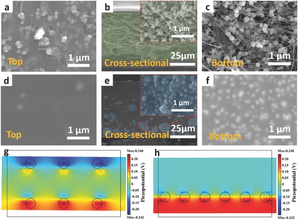
Figure 4.

SEM image of the a) top surface, b) cross‐sectional, and c) bottom surface of the BTO/BC piezoelectric paper. SEM image of the d) top surface, e) cross‐sectional, and f) bottom surface of the BTO/PDMS film. COMSOL simulation results of the output voltage of the g) BTO/BC piezoelectric paper and h) BTO/PDMS film with the compressive stress of 0.1 MPa.
