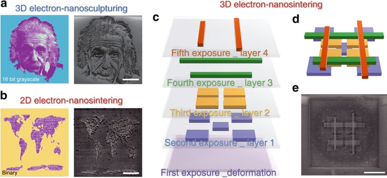
Figure 5. 2D and 3D nanostructuring of silk proteins.
(a) 3D electron-nanosculpturing: 3D nanotopographies on crystalline silk can be created using a 16-bit grayscale positive EBL (left: design image; right: SEM image). The Einstein image: Photo by Philippe Halsman @ Halsman Archive. One grayscale exposure was applied, followed by a water-only development to remove the exposed area. Scale bar, 10 μm. (b) 2D electron-nanosintering: 2D nanotopographies on amorphous silk proteins can be created using a binary negative EBL (left: design image; right: SEM image). Scale bar, 15 μm. One exposure was applied to crosslink the exposed area. Unexposed area is removed after water development. (c) 3D electron-nanosintering: 3D nanostructures on crystalline silk can be created using a LbL multi-EBL. Multiple exposures are applied in sequence to define each layer. The first exposure is to de-crosslink the crystalline silk proteins, resulting in amorphous proteins to be sintered/re-crosslinked by the following LbL EBL steps. For amorphous silk, this step (the first exposure) is unnecessary. (d) Schematic and (e) SEM images of as-designed 3D silk nanostructures using an LbL nanosintering process. Scale bar, 5 μm.

