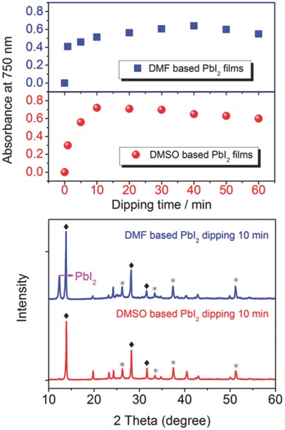
Figure 3.

a) Variation of layer absorbance at 750 nm as a function of dipping time corresponding to conventional DMF–PbI2‐based (blue) and as‐prepared DMSO–PbI2 ‐based perovskite layer (red). b) X‐ray diffraction (XRD) pattern of DMF–PbI2‐based and DMSO–PbI2‐based perovskite layer after 10 min dipping. Reproduced with permission.33 Copyright 2014, Royal Society of Chemistry.
