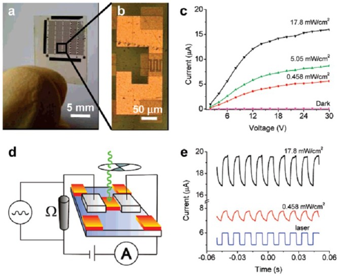
Figure 6.

Arrays of PD devices based on CdS and characterization of the photoconducting properties. a) An array of devices on the transparent flexible PET substrate. b) An optical micrograph of a single PD device. c) Dark and photocurrents at different irradiation power densities. d) Schematic diagram for the time‐dependent signal current measurement. e) On–off switching using 514‐nm laser chopped at 90 Hz. Reproduced with permission.109
