
Figure 9.
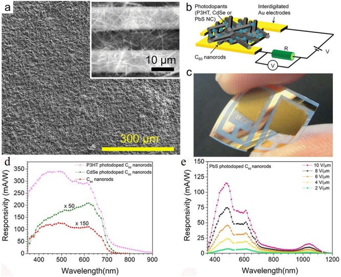
a) SEM image of a typical C60 nanorod photoconductor film. b) A schematic depicting the planar device architecture. c) Photograph of two typical C60 nanorod photoconductor devices fabricated on a flexible PEN substrate. d) Relative comparison of spectral responsivity obtained for C60 nanorod only and P3HT or CdSe NC photodoped C60 nanorod devices. e) Electric field dependent spectral responsivity of PbS NC photodoped device. Reproduced with permission.138 Copyright 2015, Macmillan Publishers Ltd.