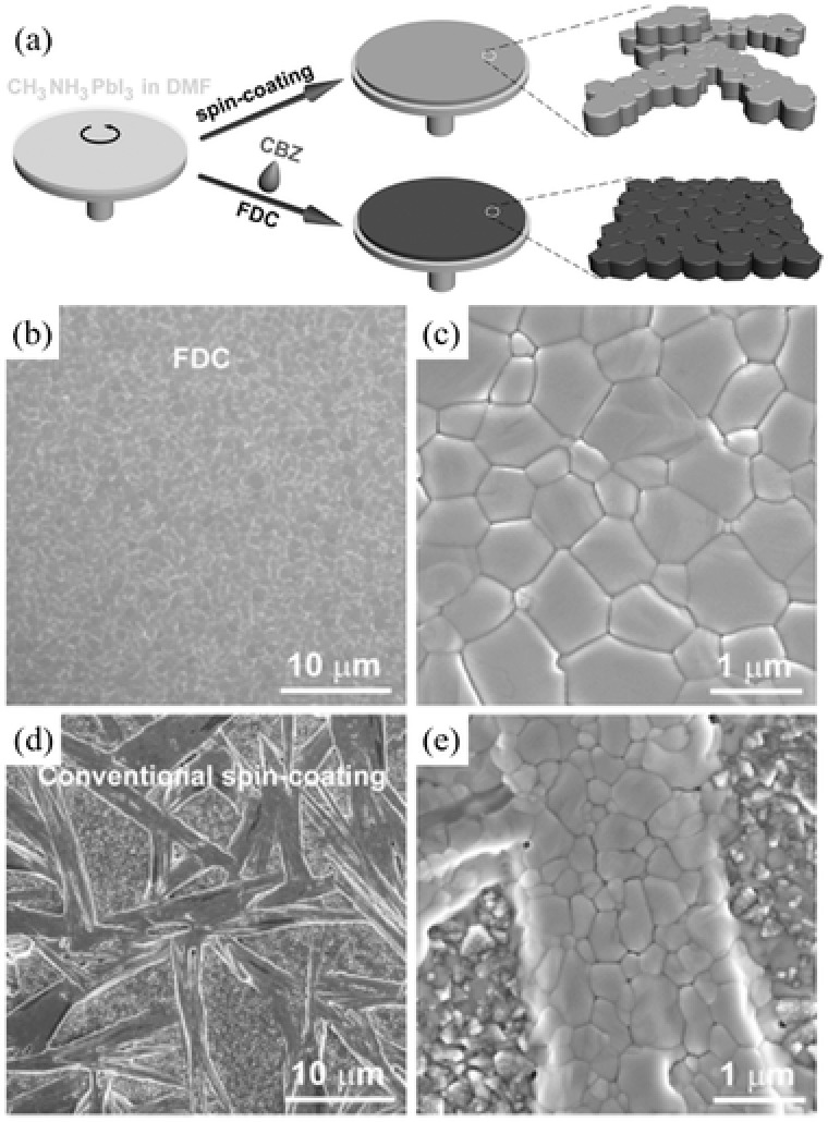
Figure 5.

a) Schematic illustration of the FDC process and conventional spin‐coating process for fabricating perovskite films. Low‐ and high‐magnification SEM images of the surface of a CH3NH3PbI3 film prepared b,c) by FDC with the addition of chlorobenzene and d,e) by conventional spin‐coating. a–e) Adapted with permission.113 Copyright 2014, WILEY‐VCH.
