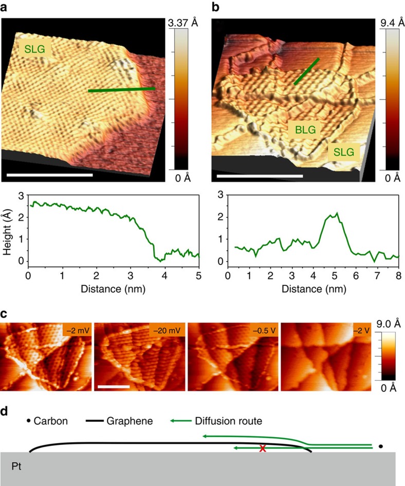
Figure 4. STM imaging of graphene edge structures.
STM images showing topographic contrast and corresponding height profiles along the green lines are shown in a,b. The images recorded at −2 mV bias voltage and 1 nA tip current show a reduced signal at the edge of single-layer graphene that is in direct contact with Pt (a) and a higher signal due to increased electron density at edge atoms terminating the top layer in BLG (b). The dependence of the topologic contrast on tip voltage at a current of 1 nA is shown in c for the case of BLG. A schematic drawing of the bonding of graphene edges and its influence on the diffusion routes of carbon species is shown in d. Scale bars in a,b,c measure 4, 20 and 10 nm, respectively.

