Fig. 2.

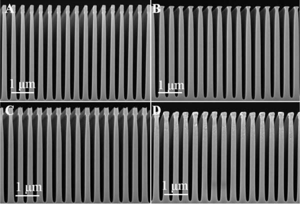
Profiles after a 2 min etch with the recipe of 1000 W ICP power, 10 W RF power, 8 mT pressure, 52 sccm SF6 and 8 sccm O2 flow rates. The mask materials are ZEP 520 (A), Cr (B), SiO2 (C) and Cr on nanoimprint resist (D).

Profiles after a 2 min etch with the recipe of 1000 W ICP power, 10 W RF power, 8 mT pressure, 52 sccm SF6 and 8 sccm O2 flow rates. The mask materials are ZEP 520 (A), Cr (B), SiO2 (C) and Cr on nanoimprint resist (D).