
Fig. 4.
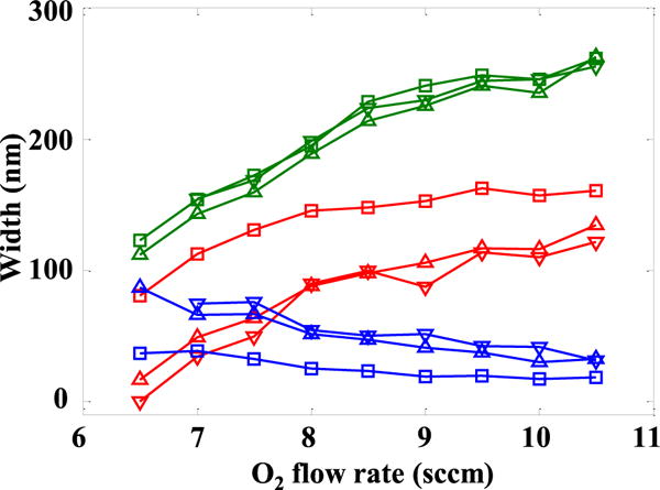
Etching characteristic widths in response to O2 flow rate for the Cr (inverted triangle), SiO2 (triangle) and Cr-on-polymer (square) masks. The blue, red and green curves represent undercut, minimum silicon width and the silicon width at half depth, respectively. The Cr masked sample did not survive 2 min etch with 6.5 sccm O2 flow rate. The minimum silicon width was taken as 0 and the other two widths are not available.