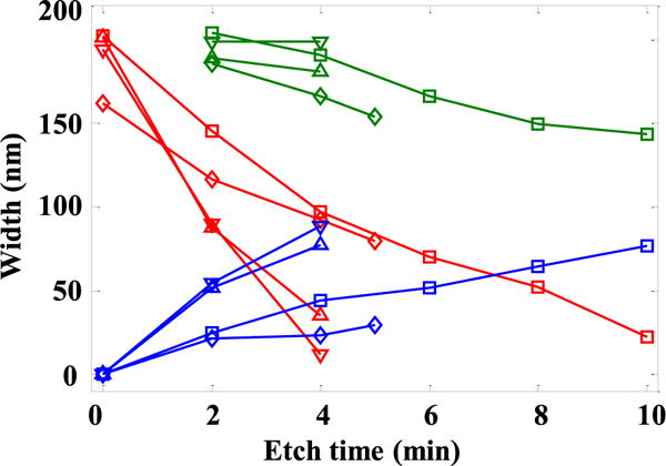
Fig. 9.

Etch characteristic widths vs the etch time for the four types of masks: ZEP 520 (diamond), Cr (inverted triangle), SiO2 (triangle) and Cr on polymer (square). The blue, red and green curves represent undercut, minimum silicon width and the silicon width at the half depth, respectively. At the start of etch the minimal silicon widths near the masks are taken as the mask widths immediately above silicon.
