
Figure 1.
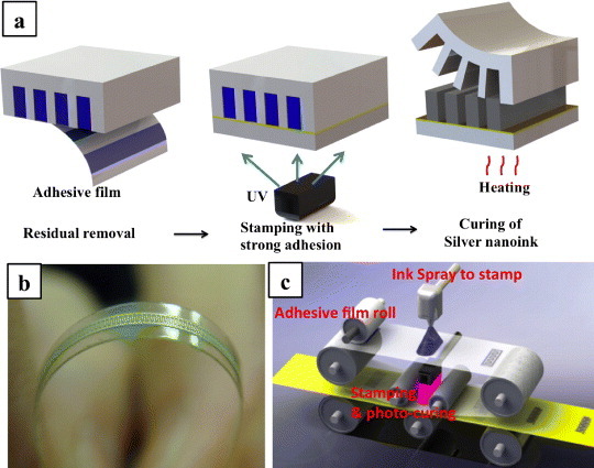
(a) Schematic of the three main steps of the direct stamping: (i) removal of AgNP residual layer (blue stripes) by an adhesive film after filling the stamp with AgNPs, (ii) UV-curing after the PDMS stamp is brought onto a substrate spread with PU prepolymer (yellow layer) and (iii) thermal curing of AgNPs after separation of the PDMS stamp. (b) Image of a sample patterned by the direct stamping method. (c) A roll-to-roll instrument designed to apply the direct stamping method to fabrication of electronic devices. Fabrication processes are continuously performed for the final product by rolls. An adhesive roll removes the residual layer after ink-spraying on a stamp, pattern is transferred on the substrate coated with a photo-curable PU layer (yellow), and then UV and heat-curing follow to finalize the product.