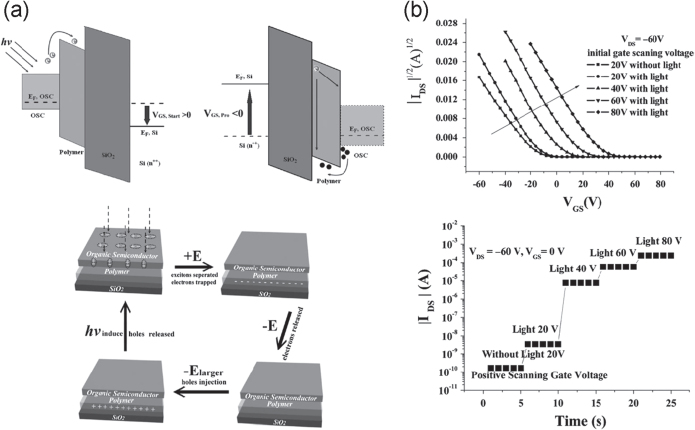
Figure 12.
(a) Energy-level diagrams to explain carrier transfer and trapping at the semiconductor–polymer interface, and illustrations of the possible mechanism of the charge generation and complexation. (b) Photo-induced variations in transistor properties and corresponding drain current levels. Reprinted from [99] with permission; © 2009 Wiley-VCH, Weinheim, Germany.

