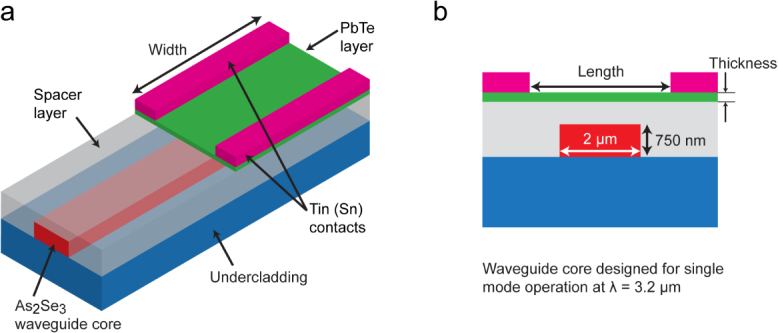
Figure 17.

(a) Integrated structure with a single-mode (λ = 3.2 μm) As2Se3 waveguide, Ge23Sb7S70 glass undercladding to prevent leakage of the mode into the Si substrate, a low index spacer to minimize modal mismatch and Fresnel reflection, and the photoconductive PbTe layer. (b) The cross-section view of the device. Reproduced with permission from [96].
