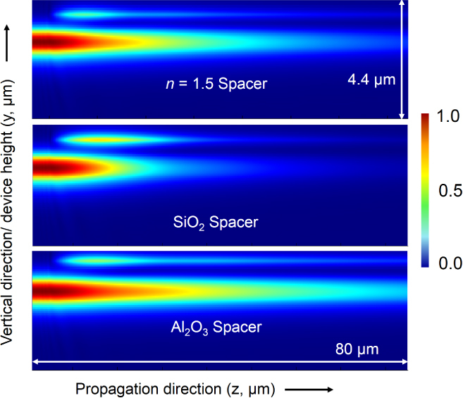
Figure 18.

3D FDTD simulations of the integrated device at λ = 3.2 μm for a 100 nm thick PbTe layer. The side (YZ) cross-section views presented for three different spacer layers exhibit the flexibility of the proposed design: all three materials allow for a gradual absorption of light in the PbTe layer with minimal reflections.
