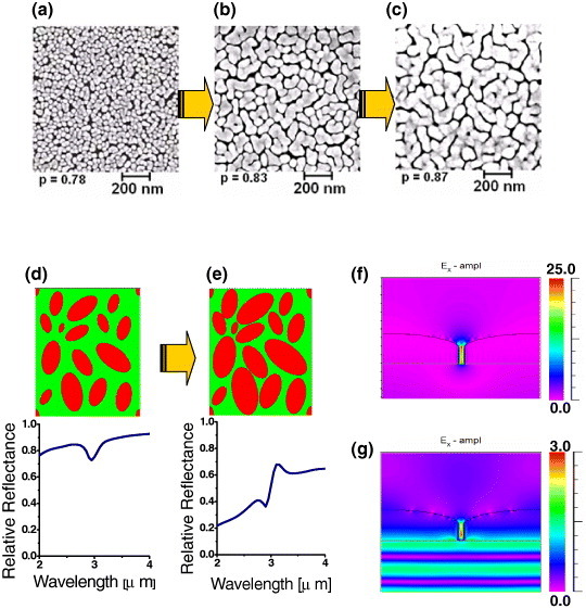
Figure 9.

(a–c) SEM micrographs of the nanogap Au island film at different growth stages; p denotes the two-dimensional filling factor of the film. (d) A model of randomly distributed islands (red ellipsoids) at the Si–water interface (220×260 nm) and its simulated reflectance spectrum. An enhanced absorption signal from the OH stretching band of water is successfully reproduced in this electromagnetic simulation. (e) A model of grown Au islands and its simulated spectrum. The simulated water absorption signal becomes asymmetric with the decrease in the average gap between the islands. (f) Simulated electric field intensity Ex (parallel to the film) near the Au nanogap (15 nm gap) upon IR illumination (wavelength 3 μm). (g) Simulated electric field intensity Ex upon visible illumination (wavelength 550 nm). The color scale shows the field intensity normalized to the incident field value.
